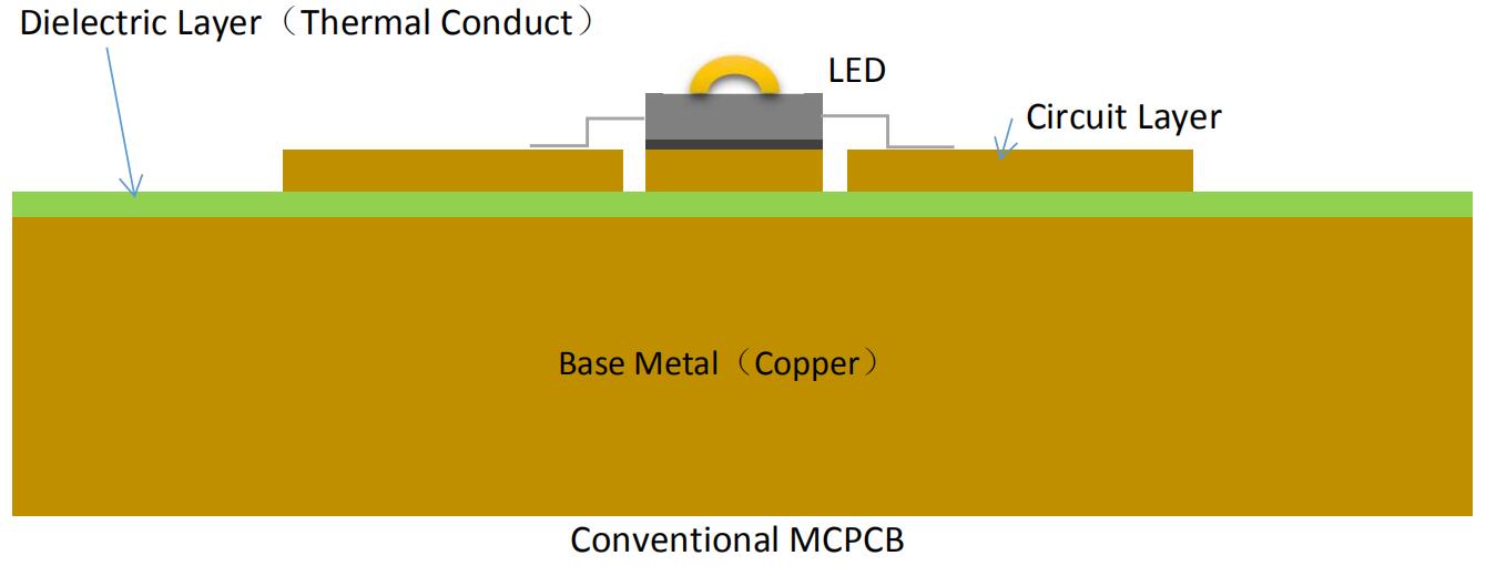
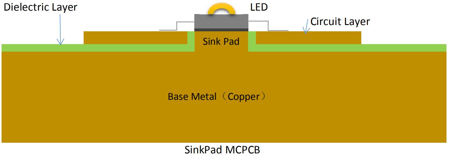
JLH TECHNOLOGY CO.,LTD's SinkPad technology:
The circuit layer and the thermal layer are on different circuit layers. The thermal layer part directly contacts the heat dissipation part of the lamp beads to achieve the best heat dissipation (zero thermal resistance), which is generally a copper base PCB.
JLH TECHNOLOGY CO.,LTD's SinkPad technology advantage:
1. Use copper base material, high density, strong heat-carrying capacity of the substrate itself, good heat conduction and heat dissipation.
2. The thermoelectric separation structure is adopted, and there is no thermal resistance in contact with the lamp beads. Minimize the luminous decay of the lamp and prolong the life of the lamp.
3. Copper substrate has high density and strong heat carrying capacity, and its volume is smaller under the same power.
4. Suitable for matching single high-power lamp beads, especially COB package, to achieve better results.
5. Various surface treatments (immersion gold, OSP, tin spray, silver plating, immersion silver + silver plating) can be performed according to different needs, and the surface treatment layer has excellent reliability.
6. According to the different design needs of the lamp, different structures can be made (copper bumps, copper recesses, thermal layer and circuit layer parallel).
Disadvantages:
Not suitable for single electrode chip bare die packaging。
JLH TECHNOLOGY CO.,LTD's SinkPad technology Steps:
1. First, cut the copper foil substrate into a size suitable for processing.
2. Note that it is usually necessary to roughen the copper foil on the surface of the board by brushing or micro-etching before pressing the substrate.
3. Adhere the dry film photoresist to the appropriate temperature and pressure. The photoresist will be polymerized after being exposed to ultraviolet light in the transparent area of the negative film (the dry film in this area will be developed and copper etched later). Lieutenant is retained as an etching resist), and the image of the circuit on the negative is transferred to the dry film photoresist on the surface of the board.
4. After tearing off the protective film on the film surface, the unexposed area of the film surface is developed and removed with an aqueous sodium carbonate solution, and then the exposed copper foil is corroded and removed with a mixed solution of hydrochloric acid and hydrogen peroxide to form a circuit.
5. Finally, the dry film photoresist is washed away with sodium hydroxide aqueous solution. For the inner layer circuit board with more than six layers (including), the automatic positioning punching machine is used to punch out the riveted reference holes for the alignment of the interlayer circuits.
We are up and running, ready to support our customers with our problem-solving LED thermal management PCBs using JLH TECHNOLOGY CO.,LTD's SinkPAD technology. We are open for business.

 EN
EN





 Whatsapp 0086 755 29438407
 Mail info@ALPCB.com
  Tel 0086 755 29438407


